Scientists began producing monocrystalline silicon nearly a century ago. Scientist Jan Czochralski discovered the modern process in 1918. However, engineers had built the first silicon solar cell by 1941. Manufacturers follow eight simple steps for this process.
Make Metallurgical Silicon
Silicon is the main material in monocrystalline panels. It comes from silica sand or quartzite (SiO2).
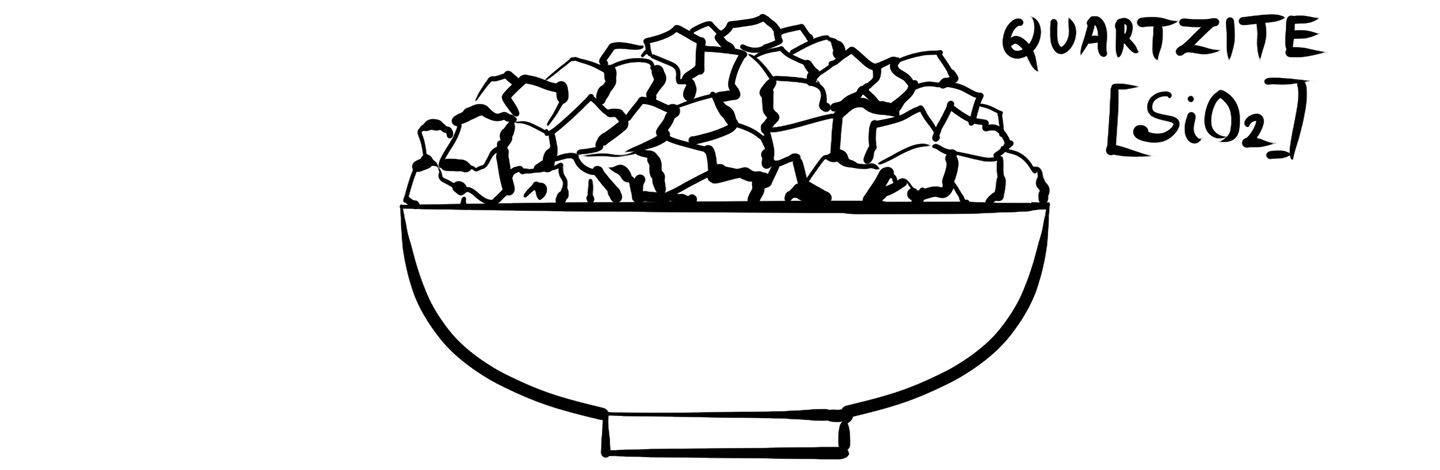
Manufacturers melt SiO2 and carbon in special ovens at over 2552°F. This process produces silicon that is 98–99% pure. However, this purity level is still not enough for solar cells. So, we must purify it further.
Purify the Silicon (Siemens Process)
The Siemens process removes impurities from metallurgical silicon. Firstly, we grind the solidified silicon into fine powder forms. Then, we react silicon powder with HCl gas inside a heated reactor. This forms trichlorosilane (SiHCl3) gas.
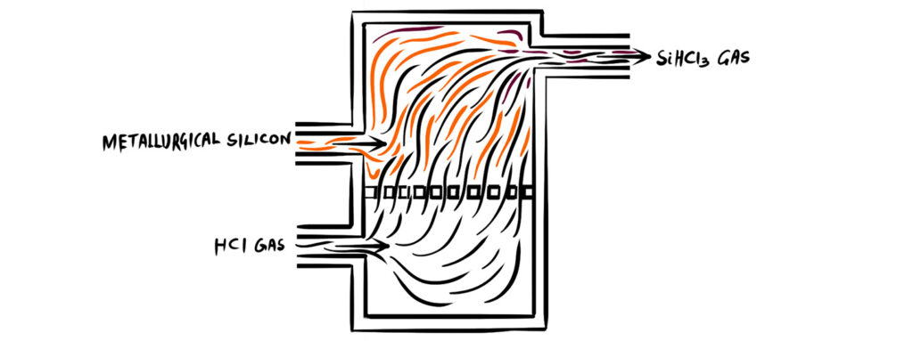
After that we cool and liquefy this gas. Then we distill it to separate unwanted elements such as calcium and aluminum. After distillation, we heat the liquid again in another reactor with hydrogen gas. High temperature breaks the chlorine bonds. Pure silicon forms on a hot rod. This method produces 99.9999% pure silicon.

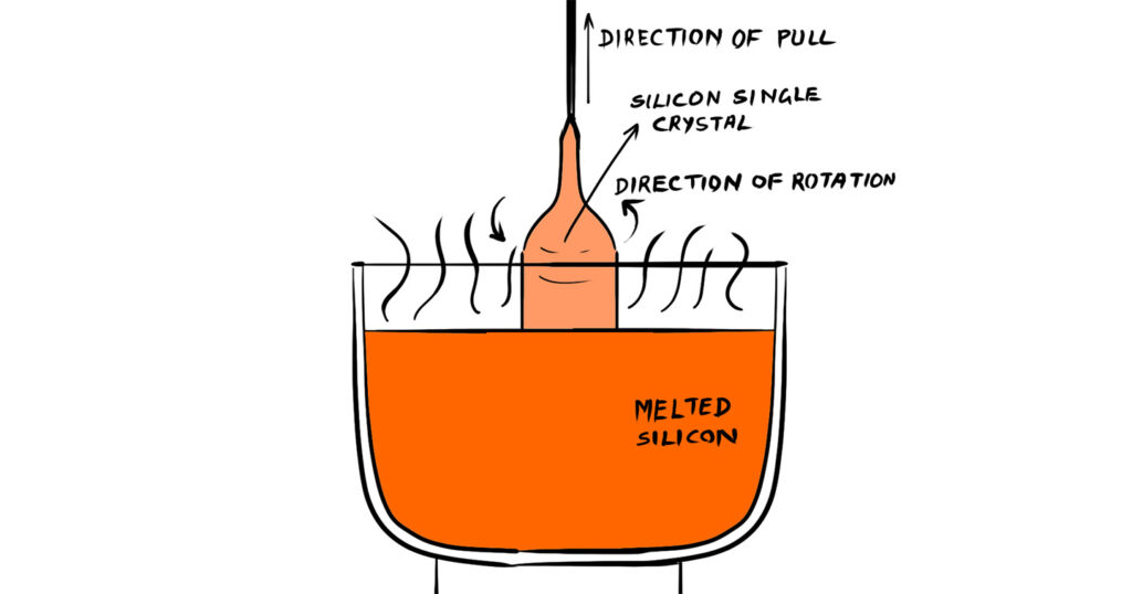
Create Silicon Ingots
Then we break and remove the pure silicon crystal from the rod. Then we again melt it. The Monocrystalline cells need a single, pure silicon crystal. We achieve this using the Czochralski method. Firstly, we dip a small seed crystal into molten silicon. Then we slowly pull and rotate the seed upward. The silicon cools and solidifies on the seed. Over several days, this forms a large, uniform cylindrical silicon ingot. Its size depends on cooling rate, temperature gradient, and rotation speed.
Slice Ingots Into Silicon Wafers
Next, we cut the ingot into thin slices. We use a sharp diamond wire saw for this. The saw produces wafers that are about 1 mm thick. We then wash and polish the wafers to remove dust, dirt, and scratches.

Improve the Wafers (Surface Texturing)
A flat wafer reflects too much sunlight. Reflection lowers solar panel efficiency. So manufacturers etch and roughen the wafer surface. Obviously, this texture traps more light by forcing it to bounce multiple times. The result is higher energy absorption and better pv cell performance.

Diffuse Phosphorus to Form a p–n Junction
Silicon wafers naturally act as p-type material. However, we need a p–n junction to generate electricity. Therefore, manufacturers add a thin phosphorus layer to create an n-type surface. The wafers then go into high-temperature ovens at 1652°F. Nitrogen and phosphorus combine to form a strong n-type layer. This step greatly improves the wafer’s ability to produce power.
Improve Conductivity (Metal Contacts)
Next, we add metal contacts to reduce electrical losses. A high-conductivity silver alloy is printed onto the front of the wafer. This silver grid collects and transports electricity efficiently. It increases the overall performance of the solar cell.

Assemble the Solar Panel
Finally, we assemble the cells into a complete panel. A monocrystalline panel contains 32 to 96 silicon cells arranged in rows and columns. Obviously, more cells mean higher power output.
