
A photovoltaic cell is nothing but a simple PN junction. There is an N-type semiconductor layer facing the sunlight. The P-type semiconductor sits below the N-type layer. Obviously, at the junction of the N and P-type semiconductors, there is a depletion layer.
Theory of Depletion Layer
The basic theory of the depletion layer at the PN junction is not within the scope of our discussion. However, let us briefly recall it.
The free electrons in the N-type layer, very near to the junction, find readily available holes in the P-type layer. As a result, these electrons and holes combine. When an electron combines with a hole, it leaves a positive ion behind. Obviously, the electrons come from the N layer and combine in the P layer. As a result, these combinations form a layer of positive ions in the junction towards the N-type semiconductor. Similarly, these electron-hole combinations create a layer of negative ions in the junction towards the P-type semiconductor. Thus, the depletion layer consists of a layer of positive ions and a layer of negative ions.
Formation of Photoelectrons
Now, suppose light falls on the N-type side. Light has photons, which are packets of energy. A photon may contain more energy than the energy gap between the valence and conduction bands of the electrons. When a photon strikes a covalent bond in the semiconductor, it can generate an electron–hole pair. Because when an electron leaves the covalent bond, it creates a hole behind.
So, the light falling on the semiconductor increases the number of free electrons. At the same time, it increases the same number of holes. Therefore, they are balanced. Obviously, that cannot create an uneven charge distribution in the semiconductor.
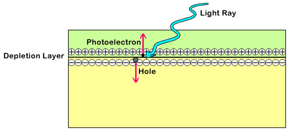
How a light Generates Potential?
But if we can manage to let the light rays enter the depletion layer, the phenomenon will be different.
In the depletion layer, there are no free electrons. As we discussed, there are only layers of negative ions and positive ions. But when the photons strike the semiconductor in the depletion layer, they will create electron–hole pairs there for the same reason. However, here, the layer of negative ions repels the photo electrons due to its electrostatic force. As a result, the electron propagates and comes out from the depletion layer, crossing the layer of positive ions, into the entire N-type substrate. Actually, due to photon strikes in the depletion layer, the generated electrons (photoelectrons) will propagate to the N-type layer very fast. So they will not have enough time to recombine.
Similarly, the photo-generated holes in the depletion layer move down to the P-type layer very fast. This is due to the repulsion by the layer of positive ions.
Photovoltaic Cell (PV Cell)
In this way, the number of free electrons increases in the N-type region. Obviously, it will continue as long as the light falls at the PN junction. Due to this uneven distribution of electron concentration, the semiconductor block will generate a potential across it. This potential is 0.6 to 0.7 volts. This is the basic structure of a PV cell.
Now, if we increase the surface area of the semiconductor block, the current (meaning the number of photo-generated electrons) will increase accordingly. If we connect many such blocks in series, we can increase the output voltage. This adds up the voltage of each PV cell.
There is a main constructional feature that differentiates a PV cell from a normal PN diode. A PV cell has a very thin layer of N-type substrate, so that the light can easily hit the junction.
This is the simple and basic working principle of a photovoltaic cell.